


A silicon photodiode is a solid-state device which converts incident light into an electric current. It consists of a shallow diffused p-n junction, normally a p-on-n configuration although “P-type” devices (n-on-p) are available for enhanced responsivity in the 1µm region. Modern day silicon photodiodes are generally made by planar diffusion or ion-implantation methods.
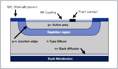
In the p-on-n planar diffused configuration, shown in the figure, the junction edge emerges on the top surface of the silicon chip, where it is passivated by a thermally grown oxide layer.
BASIC PHOTODIODE PHYSICS
The p-n junction and the depletion region are of major importance to the operation of a photodiode. These photodiode regions are created when the p-type dopant with acceptor impurities (excess holes), comes into contact with the n-type silicon, doped with donor impurities (excess electrons). The holes and the electrons, each experiencing a lower potential on the opposite side of the junction, begin to flow across the junction into their respective lower potential areas. This charge movement establishes a depletion region, which has an electric field opposite and equal to the low potential field, and hence no more current flows.
When photons of energy greater than 1.1eV (the bandgap of silicon) fall on the device, they are absorbed and electron-hole pairs are created. The depth at which the photons are absorbed depends upon their energy; the lower the energy of the photons, the deeper they are absorbed. The electron-hole pairs drift apart, and when the minority carriers reach the junction, they are swept across by the electric field. If the two sides are electrically connected, an external current flows through the connection. If the created minority carriers of that region recombine with the bulk carriers of that region before reaching the junction field, the carriers are lost and no external current flows.
The equivalent circuit of a photodiode is shown in the figure below. The photodiode behaves as a current source when illuminated. When operated without bias, this current is distributed between the internal shunt resistance and external load resistor. In this mode, a voltage develops which creates a forward bias, thus reducing its ability to remain a constant current source. When operated with a reverse voltage bias, the photodiode becomes an ideal current source.
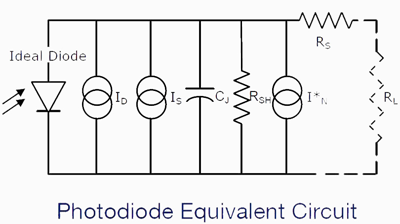
| ID | = | Dark current, Amps |
| IS | = | Light Signal Current (IS=RPO) |
| R | = | Photodiode responsivity at wavelength of irradiance, Amps/Watt |
| PO | = | Light power incident on photodiode active area, Watts |
| RSH | = | Shunt Resistance, Ohms |
| I*N | = | Noise Current, Amps rms |
| C | = | Junction Capacitance, Farads |
| RS | = | Series Resistance, Ohms |
| RL | = | Load Resistance, Ohms |
Silicon photodiodes are typically sensitive to light in the spectral range from about 200 nm (near UV) to about 1100 nm (near IR). Photosensor responsivity (R) is measured in Amperes (A) of photocurrent generated per Watt (W) of incident light power. Actual light levels in most applications typically range from picoWatts to milliWatts, which generate photocurrents from pico-Amps to milli-Amps. Responsivity in Amps/Watt varies with the wavelength of the incident light, with peak values from 0.4 to 0.7 A/W. The silicon photodiode response is well matched to light sources emitting in the UV to near infrared spectrum, such as HeNe lasers; GaAlAs and GaAs LEDs and laser diodes; and Nd:YAG lasers. Select a detector from the IR, Blue/Visible or UV series for a spectral response curve best matched to the spectral irradiance of your light source.
The silicon photodiode response is usually linear within a few tenths of a percent from the minimum detectable incident light power up to several milliWatts. Response linearity improves with increasing applied reverse bias and decreasing effective load resistance.
Heating the silicon photodiode shifts its spectral response curve (including the peak) toward longer wavelengths. Conversely, cooling shifts the response toward shorter wavelengths. The following values are typical for the temperature dependence of responsivity for different wavelength regions:-
UV to 500nm: -0.1%/°C to -2%/°C
500 to 700nm: ~0%/°C
~900nm: 0.1 %/°C
1064 nm: 0.75%/°C to 0.9%/°C
MODES OF OPERATION
A silicon photodiode can be operated in either the photovoltaic or photoconductive mode. In the photovoltaic mode, the photodiode is unbiased; while for the photoconductive mode, an external reverse bias is applied. Mode selection depends upon the speed requirements of the application, and the amount of dark current that is tolerable. In the photovoltaic mode, dark current is at a minimum. Photodiodes exhibit their fastest switching speeds when operated in the photoconductive mode.
Photodiodes and Op-Amps can be coupled such that the photodiode operates in a short circuit current mode. The op-amp functions as a simple current to voltage converter.